Quick Answer
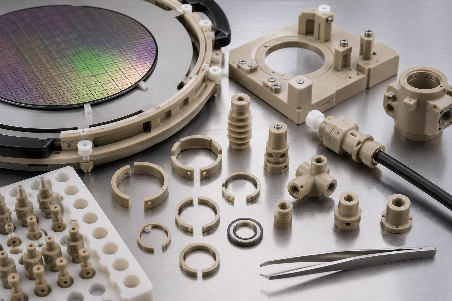
PEEK supports selected semiconductor components that demand heat and chemical resistance, dimensional stability, wear performance, electrical insulation, cleanliness, and low outgassing.
What PEEK Is
PEEK, or polyetheretherketone, is a semi-crystalline high-performance engineering thermoplastic used when a component must retain useful mechanical, dimensional, thermal, or chemical performance under demanding service conditions. It is commonly supplied as sheet, plate, rod, tube, and precision-machined components.
Unfilled, glass-filled, carbon-filled, bearing-grade, medical-grade, and other specialized PEEK formulations can perform differently. Material selection should therefore be based on the exact grade, operating environment, finished-part design, and documentation requirements.
Key Properties and Performance Factors
Semiconductor production environments require materials that can withstand:
- Aggressive process chemicals
- High operating temperatures
- Vacuum conditions
- Cleanroom requirements
- Tight dimensional tolerances
- Continuous mechanical wear
PEEK maintains its performance under these demanding conditions while minimizing contamination risks that can negatively impact wafer yields and production efficiency.
- High continuous-use temperature capability
- Excellent chemical resistance
- Low moisture absorption
- Low outgassing characteristics
- Exceptional wear resistance
- Tight tolerance capability
- Long service life
- Reduced particle generation
- Excellent dimensional stability
These characteristics help improve equipment reliability, reduce maintenance requirements, and support the stringent cleanliness standards required throughout semiconductor manufacturing.
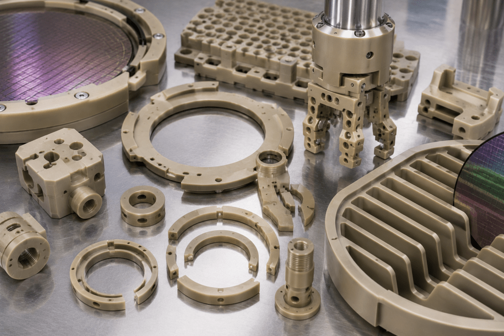
Wear resistance and dimensional control make PEEK useful in selected CMP and wafer-handling roles.
Common Applications in Semiconductor Manufacturing
CMP Retaining Rings
Chemical Mechanical Polishing (CMP) systems use retaining rings to control wafer positioning during polishing operations. PEEK’s excellent wear resistance and dimensional stability help extend component life and maintain process consistency.
Wafer Handling Components
PEEK is commonly used for:
- Wafer carriers
- Wafer cassettes
- Process trays
- End effectors
- Robotic handling components
Its combination of strength, cleanliness, and dimensional stability helps protect sensitive wafers throughout the manufacturing process.
Fluid Handling Systems
PEEK components are frequently found in:
- Manifolds
- Valves
- Fittings
- Pump components
- Chemical delivery systems
Its resistance to many acids, solvents, and process chemicals makes it suitable for demanding wet-processing environments.
Electrical Insulators
PEEK provides excellent electrical insulation and thermal stability, making it useful for:
- Insulating rings
- Connector bodies
- Sensor housings
- Electronic support structures
- Test socket components
These applications benefit from PEEK’s ability to maintain electrical performance at elevated temperatures.
Vacuum and Process Equipment
Many semiconductor processing tools operate under vacuum conditions where low-outgassing materials are essential. PEEK is often used in vacuum-compatible components because it generates minimal contamination and maintains stability during thermal cycling.
Important Selection Considerations for PEEK semiconductor applications
- Review process chemistry, temperature, vacuum, plasma, and mechanical wear conditions by tool location.
- Confirm grade-specific purity, particle, extractables, outgassing, and cleanroom requirements.
- Evaluate electrical insulation or static-control requirements because filled and conductive grades behave differently.
- Define critical tolerances, inspection methods, traceability, and change-control expectations before production.
Engineers and purchasing teams should also consider total cost of ownership. A material and grade that machine predictably, hold appropriate tolerances, and perform consistently in the actual environment can reduce downtime, premature wear, rework, and replacement cost.
Comparisons and Alternatives
In semiconductor equipment, PEEK may be compared with PPS, PAI, ULTEM™ PEI, PTFE, PFA, PVDF, ceramics, or quartz. The best fit depends on process chemistry, plasma exposure, heat, vacuum, cleanliness, static control, dimensional stability, and total cost of ownership.
Fabrication, Machining, and Documentation Notes
PEEK machines well, but its material cost and performance expectations make drawing review and process planning especially important. Thin walls, deep pockets, sharp internal corners, large cross sections, aggressive tolerances, and unbalanced stock removal can affect final part stability.
Production drawings should identify the exact grade, critical dimensions, surface finish, holes, threads, sealing features, inspection methods, and documentation requirements. Manufacturer, lot traceability, certificates, test reports, and customer-specific quality expectations should be discussed before material is released.
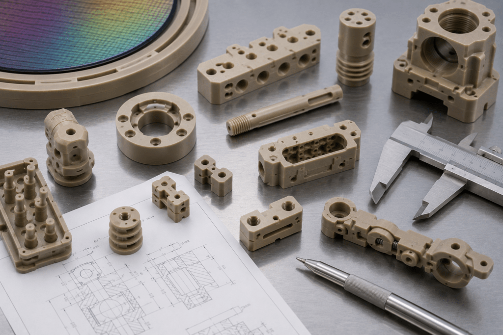
PEEK may support electrical, vacuum, and fluid-management functions when grade-specific cleanliness is verified.
Why Modern Plastics
Modern Plastics supplies PEEK stock shapes and precision-machined PEEK components for semiconductor equipment manufacturers, OEMs, and fabrication facilities. Common applications include CMP retaining rings, wafer handling components, fluid management systems, insulators, and custom-machined semiconductor equipment parts.
When evaluating semiconductor materials, PEEK is often compared with PPS, PTFE, PVDF, ULTEM™, and ceramic materials to identify the optimal balance of performance, cleanliness, manufacturability, and cost for the specific application.
Is PEEK the Right Material for Semiconductor Manufacturing?
PEEK semiconductor applications can be a strong fit when the application requires a demanding combination of thermal performance, mechanical strength, dimensional stability, chemical resistance, wear performance, or electrical insulation. PEEK is not automatically the best or most economical choice for every part, so the exact grade and alternatives should be compared against the real service conditions before a final specification is approved.
Frequently Asked Questions About PEEK for Semiconductor Manufacturing Applications
Where is PEEK used in semiconductor manufacturing?
PEEK is used in selected CMP retaining rings, wafer-handling components, process trays, end effectors, manifolds, valves, fittings, insulators, test fixtures, and vacuum-compatible process-tool components.
Why is PEEK considered for CMP retaining rings?
PEEK offers wear resistance, dimensional stability, strength, and machinability that can support controlled wafer positioning and repeatable polishing performance. The precise grade and cleanliness requirements should be matched to the tool.
Is all PEEK low outgassing and cleanroom suitable?
No. Outgassing, extractables, particle behavior, purity, additives, and processing history can differ by grade and supplier. Use grade-specific test data and application qualification rather than a generic material assumption.
What materials compete with PEEK in semiconductor equipment?
Depending on chemistry, plasma, temperature, purity, static control, and cost, alternatives may include PPS, PTFE, PFA, PVDF, ULTEM™ PEI, PAI, specialty composites, ceramics, or quartz.
Can Modern Plastics support machined PEEK semiconductor parts?
Yes. Modern Plastics supplies high-performance stock shapes and supports precision-machined components, material review, documentation, and sourcing for semiconductor equipment applications.
Talk to Modern Plastics About Your Application
Whether you need help choosing the right plastic material, comparing performance properties, improving manufacturability, reviewing documentation requirements, or sourcing stock shapes and fabricated components, the Modern Plastics team is ready to help.
0 Comments